

Siglent STB-3 Oscilloscope Demo / Training Board


Siglent STB3 Demo Board
A versatile multi-signal source designed to demonstrate and test Siglent oscilloscopes. Generates analog, digital, and serial protocol signals including I²C, SPI, UART, LIN, and CAN. Ideal for education, oscilloscope training, and feature demonstrations.
A board that misbehaves on purpose
Learning what an oscilloscope can really do is awkward, because the interesting features exist for signals you do not have to hand. Glitch trigger needs a glitch. Runt trigger needs a runt. Enhanced-resolution mode only proves itself on something genuinely noisy. Waiting for a real circuit to misbehave is not a teaching plan.
The STB3 generates all of them deliberately, to known figures. Sixteen analogue and pulse signals from a 25 MHz sine down to a 60 ns glitch buried in a pseudo-noise stream, plus five serial buses — I²C, SPI, UART, LIN and CAN — each carrying a payload you already know, so a decode that comes out wrong is obvious at a glance.
It runs from a USB cable. There is no software, no mains adaptor and nothing to configure: press a button to pick a signal group and probe the jumper or the BNC. Equally useful for a training room, for evaluating an instrument before you buy it, and for checking that a probe and its ground lead are doing what you think.
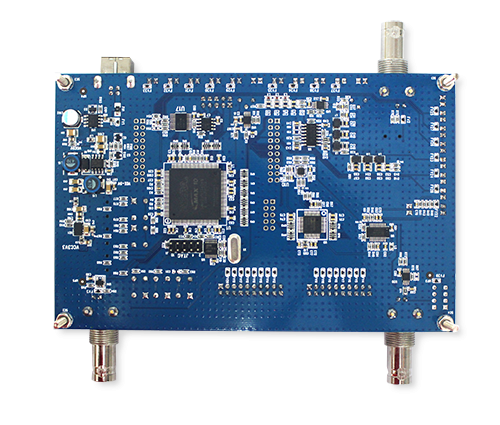
The everyday waveforms
Eight standard signals with published amplitudes and offsets, so a measurement can be checked against a number rather than an impression.
| Signal | Specification | What it is for |
|---|---|---|
| Sine wave 1 | 25 MHz · ~1.3 Vpp | From the jumper. Fast enough to show where a probe's bandwidth and loading start to matter. |
| Sine wave 2 | 1.25 MHz · ~750 mVpp | From the BNC connector — the everyday reference signal for probe compensation and basic measurement. |
| Square wave 1 | 1 kHz · ~3 Vpp, 3.3 V offset | The classic probe-compensation square. |
| Square wave 2 | 100 kHz · ~3.3 Vpp, 1.7 V offset | Mid-speed edges for timing work. |
| Square wave 3 | 10 MHz · ~3.3 Vpp, 1.7 V offset | Fast enough that the ground lead changes the answer — use the ground spring, which is the lesson. |
| AM signal | 25 MHz carrier, 2.5 MHz modulation | Adjustable modulation depth, for envelope and modulation-domain demonstrations. |
| Fast-edge square | 1 MHz and 10 Hz, LVPECL | Manually triggered. An LVPECL edge for rise-time and bandwidth checks. |
| Burst | 500 ns pulses · 1, 10 or 100 | Manually triggered, for burst and N-edge trigger practice. |
The awkward ones
Each of these exists to exercise one trigger or acquisition mode. This is the part of the board you cannot easily reproduce with a signal generator.
PWM
24.4 kHz carrier with the duty cycle sweeping 25% to 50% — a moving target for pulse-width trigger and measurement.
Burst
~65 ms period, 500 ns pulses, for interval and timeout triggering.
Glitch
A 1 Mbps pseudo-noise stream carrying a 60 ns, 1.6 V glitch every 15 ms. The classic case for glitch trigger — and a reminder that probe loading changes what you see, because the source impedance is high.
Slope
A 156 kHz square whose falling edge has a 200 ns step added, giving an effective negative slope of about 200 ns for slope/rise-time triggering.
Runt
A 300 ns runt pulse appearing in the 1 Mbps stream every 6.3 ms at most — the pulse that fails to reach a full logic level.
Pseudo-noise sequence
A plain 1 Mbps pseudo-random stream, useful as a realistic background for search, zoom and history.
Noisy PWM
1.5 kHz carrier, duty cycle 25–50%, with adjustable noise — built specifically to demonstrate ERES (enhanced resolution) acquisition.
SPO demonstration signal
A complex waveform designed to show intensity grading on a Super Phosphor display. Needs a considered trigger setup, which is part of the point.
Five serial buses
Every I²C, SPI and UART transfer carries the same twelve bytes — the ASCII text SIGLENT_ followed by four random characters. Knowing what the payload should say is what makes this a teaching tool rather than just a signal source.
| Bus | Rate | Configuration |
|---|---|---|
| I²C | 100 kbps | 7-bit and 10-bit addressing, read and write, four different frame types |
| SPI | 1 Mbps | CPOL=1, CPHA=1 · 8-bit · MSB first · active-low chip select |
| UART | 9.6 kbps | Idle high · 8-bit · MSB first · odd parity · 2 stop bits |
| LIN | 9.6 kbps | LIN 2.0 framing — break, sync, PID, data and checksum |
| CAN | 50 kbps | Extended format, ISO 11898-5 physical layer |
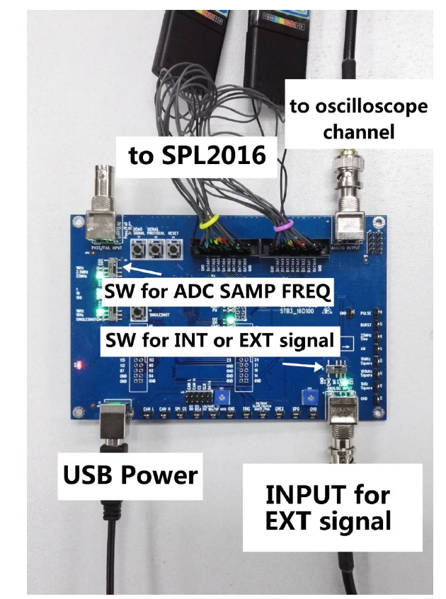
Mixed-signal and pass/fail demonstrations
MSO demonstration
The board digitises an analogue signal on its own ADC and presents the result on the digital header, so an analogue trace and the digital word describing it can be compared side by side. You can feed it the onboard 1.25 MHz sine or your own external signal, take the buffered analogue output from the BNC, and switch the sampling rate between 1, 2.5 and 25 MSPS — which makes aliasing something you can show rather than describe. Documented against the SDS2000X and the SPL2016 logic probe, and usable with other Siglent MSO models.
Pass/fail demonstration
A BNC input takes the oscilloscope's pass/fail output. When a failure occurs the onboard LED flickers once, so mask testing becomes visible in the room instead of a counter changing on a screen. Documented against the SDS2000X pass/fail output.
Manual
Every figure on this page comes from the user manual, which also has an oscilloscope screenshot of each signal and the connection diagrams.
All signal specifications, a screenshot of each waveform, the serial frame tables and the connection examples.
Questions we are asked
What is the STB3 for?
Producing known, repeatable signals so you can learn or demonstrate an oscilloscope's advanced functions without hunting for a real circuit that misbehaves on cue. It generates the awkward cases on purpose: glitches, runts, slow edges, noisy PWM and five serial buses.
Which oscilloscopes does it work with?
Any oscilloscope — the outputs are ordinary signals on a BNC and on jumpers. The manual documents the PASS/FAIL and MSO demonstrations against the SDS2000X and the SPL2016 logic probe, and notes they can be used with other Siglent MSO models.
What does it need to run?
A USB cable for power, and nothing else. There is no mains adaptor and no software to install.
Can I use it to check a probe?
Yes, and it is one of the better uses. The 1 kHz square is the standard compensation signal, and the 10 MHz square shows what a long ground lead does to a fast edge — the manual specifically tells you to use a ground spring on that one.
Does it decode the serial buses itself?
No — it generates them. The decoding happens in the oscilloscope, which is the point: the board gives you a known-good I²C, SPI, UART, LIN or CAN stream so you can practise setting up decode and triggering and check your result against a payload you already know.
What is actually in the serial data?
Each I²C, SPI and UART transfer carries the same 12 bytes — the ASCII text SIGLENT_ followed by four random characters. Because you know what it should say, a decode that comes out wrong is immediately obvious.
Goes with
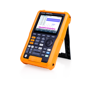
Handheld oscilloscopes with the serial decoding this board exercises.
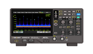
12-bit entry oscilloscopes — decode and Bode plot standard.
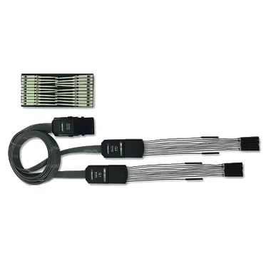
16-channel logic probe, used in the board's MSO demonstration.
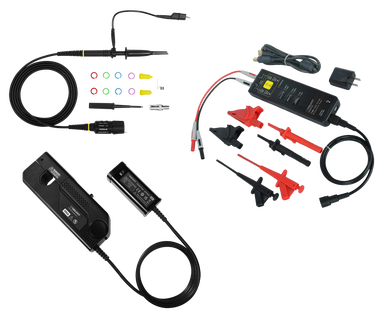
Passive and active probes — the board is a good way to compare them.
Teaching, evaluating or demonstrating?
Tell us what you need to show and on which instrument, and we will confirm the board covers it. Useful in quantity for training rooms — ask us about multiples. We are the official Siglent distributor for the European Union.